Compared with the existence of human civilization for thousands of years, the history of the discovery of graphene, a thin two-dimensional material, is undoubtedly short, but its wonderful physical properties have attracted the attention of researchers. Since the production of single-layer graphene by Andre Heim's team in Manchester in 2004, a series of properties of graphene have been continuously discovered, such as carrier mobility-theoretical value of 1 million square centimeters·V^ -1 · second^ -1 (cm ^ 2·V ^ -1·s ^ -1), anti-major quantum Hall effect, room temperature quantum Hall effect, mass Dirac fermion behavior, and mechanical strength and thermal conductivity , Excellent light transmittance and conductivity, specific surface area, etc. These excellent properties make graphene have broad application prospects in the fields of microelectronics, sensors and biomedicine, so graphene is also called "black gold". Nowadays, the R&D competition of graphene and other two-dimensional materials and devices is becoming increasingly fierce. The international semiconductor technology roadmap has listed graphene and other two-dimensional materials as new materials that are expected to continue Moore's law, and are widely used in integrated circuits and new nanoelectronic devices. . In the future, two-dimensional nanoelectronic devices composed of two-dimensional crystals are expected to bring about changes in microelectronics technology, and may even shake the silicon-based microelectronic devices dominated by integrated circuits for half a century, and are widely used in people’s daily lives. In life. Boron Nitride

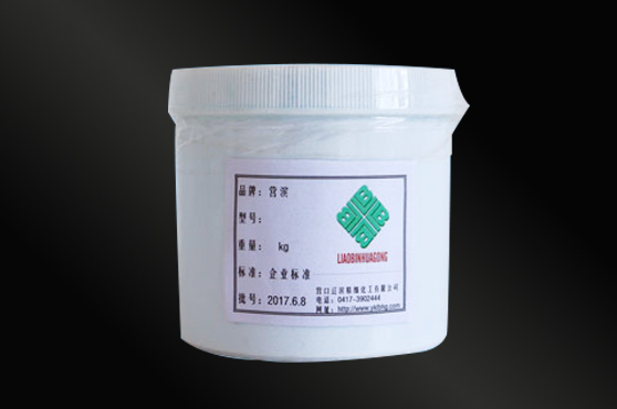
Two-dimensional materials represented by graphene are full of opportunities in the process of replacing traditional semiconductor materials in the field of microelectronics and application in large-scale integrated circuit manufacturing. At the same time, they are also facing many major scientific problems that need to be solved urgently. For example, the preparation and application of graphene microelectronic devices require high carrier mobility, suitable band gap, low intracrystalline defects, flat surface, low charge impurity concentration, uniform dielectric coverage, and so on. Faced with the above problems, hexagonal boron nitride (h-BN) is currently a kind of graphene device edge substrate. The hexagonal boron nitride body material and graphite are isoelectronic bodies, with a similar layered structure, white in appearance, and commonly known as "white graphite". It has the same layered hexagonal plane structure as graphene, has an atomic level flat surface, no dangling bonds on the surface, and has a lattice mismatch of 1.8% with graphene. It has weak doping effect and can maintain graphite. Intrinsic physical properties of alkenes. It has been reported that after transferring graphene to a hexagonal boron nitride substrate, the measured electron mobility is an order of magnitude higher than that obtained on the surface of silicon dioxide. However, most of the hexagonal boron nitride films prepared by chemical vapor deposition are a single layer composed of small crystal domains, and the preparation technology of large-area uniform multi-layer boron nitride films has not yet been achieved.
In response to the above scientific issues, the research team of the Shanghai Institute of Microsystems and Information Technology has carried out research on the heterostructure and device applications of "black gold" graphene and "white graphite" hexagonal boron nitride materials, and has achieved a series of significant achievements. Research progress.

Telephone: 15940764666
Landline: 0417-3902111
Website: www.yklbhg.com
Address: No. 517, Xiangyang Chemical Industry Park, Laobian District, Yingkou City, Liaoning Province
Landline: 0417-3902444
Fax: 0417-3902118
Mail box: 758007001@qq.com
Address: No. 517, Xiangyang Chemical Industry Park, Laobian District, Yingkou City, Liaoning Province
